Hey folks, let’s cut to the chase here – if you’re in the electronics game, you know leaded ceramic packages aren’t just a “box” for your semiconductors. They’re the unsung heroes that keep chips safe, stable, and kicking in everything from medical devices to industrial gear. As a leaded ceramic packages supplier, I field this question every single day: why do leaded ceramic packages cost what they do? I get it, margins are tight, and every dollar counts – but there’s a lot more going into the price tag than meets the eye. Today, I’m pulling back the curtain on the real cost factors that drive our quotes, so you can make smarter buying decisions without pulling your hair out. Let’s dive in. Leaded Ceramic Packages
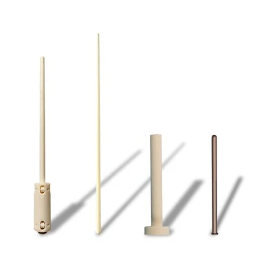
First off, let’s talk material science – because this stuff isn’t made from your grandma’s pottery clay. Leaded ceramic packages use specialized ceramic materials, most commonly alumina (Al2O3) or aluminum nitride (AlN), right? Wait, before you zone out, hear me out – not all alumina is created equal. If you need a package that can handle high power or extreme temps, you’re going to shell out for high-purity alumina (96% or higher) instead of the low-grade 85% stuff. Why? Higher purity means better thermal conductivity, less risk of cracking when you’re soldering or the device’s running hot, and more consistent electrical performance. For a lot of our clients – think aerospace or medical sensor makers – that reliability isn’t a “nice to have” – it’s non-negotiable.
Then there’s the actual metal lead frames and termination layers. We use things like tungsten, molybdenum, gold, and nickel here – and these materials have skyrocketed in price lately. Gold, for example, saw a huge jump in 2023 because of global economic uncertainty, and tungsten isn’t cheap either – it’s a rare metal used in everything from lightbulbs to fighter jets, so supply chains are tight. If a client needs gold plating for better corrosion resistance or wire bonding, that adds a premium. If they can get away with nickel-palladium gold (ENIG) instead of solid gold, that cuts costs a bit, but it’s a case-by-case thing based on their application.
Next up: manufacturing processes. This is where the rubber meets the road, and where a lot of hidden costs live. Leaded ceramic packages go through a ton of precise steps – punching, printing, firing, plating, packaging. Firing, for example, requires high-temperature furnaces that run at 1,500°C or more. Those furnaces aren’t cheap to buy, and they eat up so much energy that a single firing cycle can cost hundreds of dollars. And if you mess up the firing temperature or atmosphere (you need a precise mix of nitrogen and hydrogen to avoid oxidation), you’ve got a whole batch of cracked or discolored packages that are useless. That’s rework or scrap cost that gets passed on – no way around it.
Then there’s the lead frame formation. We punch or etch the metal lead frames to super tight tolerances – like within a few thousandths of an inch. If the leads are even a little off, they won’t line up with your chip’s contacts, and you can’t assemble the device. Etching is more precise than punching, especially for small, complex packages, so that’s another cost driver. And don’t get me started on plating – we have to plate the leads evenly so there’s no bare metal that would corrode or fail. It’s a multi-step process, and if one part of the lead is under-plated, that package is trash. Scrap rate is a big one here – our average scrap rate is around 2-3%, but if a client has a really custom design with tiny leads, that scrap rate can jump to 5-7%, and that gets factored into the per-unit price.
Customization is another huge cost factor, and I can’t stress this enough. Not every leaded ceramic package is the same. Some clients need standard 8-lead DIP packages for old designs, but most of the time, we’re making something one-of-a-kind. Maybe they need a package with a special shape to fit a new sensor, or lead counts that don’t exist in standard catalogs, or a specific cavity size to hold a large die. Custom tooling for punching or etching those lead frames isn’t cheap – a single custom tool can run $5,000 to $20,000, depending on complexity. And if you need a special finish or a custom marking (like a part number or logo), that’s extra time and materials. The kicker? For small batches, the tooling cost gets spread over fewer units, so per-unit prices go way up. For example, a standard 1000-unit order of a standard DIP package might be $0.50 each, but a custom 500-unit order of a weird leaded package could be $5 each – that’s a 10x difference, all because of tooling and customization.
Lead time also ties into costs, which I know isn’t exactly a “cost factor” you see listed on quotes, but it’s super important. If a client needs a rush order – like, 2 weeks instead of 8 – we have to push other orders to the side, assign more operators to your batch, maybe run an extra furnace cycle that wasn’t scheduled. That rush fee isn’t just us being lazy – it’s actual extra labor and production costs. We also have to order materials faster, which might mean paying a premium for expedited shipping from our metal suppliers. So if you can plan ahead, you’ll save money – that’s a tip I give every new client.
Quality assurance (QA) and compliance are non-negotiable, and they add up. For industries like medical, aerospace, or automotive, every single package has to be tested for things like hermeticity (no air or moisture getting inside), thermal performance, and electrical continuity. We use things like fine leak testing (with helium, which is expensive) and X-ray inspection to make sure there are no hidden defects. Plus, we have to meet industry standards like ISO 9001, IPC-9701, or aerospace specs like AS9100. That means extra staff for QA, extra testing equipment, and lots of paperwork to prove we’re compliant. For a client that needs parts with full traceability (every batch, every material source tracked), that’s a lot of extra work that gets passed on.
Raw material availability is another big one, and the last couple years have been wild. Things like alumina powder and tungsten metal have had supply chain issues due to things like shipping delays, geopolitical tensions, and raw material shortages. When supply is tight, prices go up, and we can’t just switch to a cheaper alternative – because our clients’ applications depend on the material’s properties. For example, during the 2022 alumina shortage, we had to lock in multi-year contracts with our suppliers to keep material prices stable, which meant we had to raise our quotes temporarily. It’s not ideal, but it’s how we keep our clients from getting hit with surprise price hikes.
Wait, let’s not forget labor. This isn’t fully automated production (yet). There’s a lot of skilled work that goes into each step – operators who know how to adjust the furnace temperature perfectly, QA techs who can spot a tiny defect under a microscope, engineers who design custom packages. Skilled labor isn’t cheap, especially in places where we do our manufacturing (I won’t name locations, but they’re areas with high demand for technical workers). And because leaded ceramic packages are precision parts, we can’t use unskilled labor – one wrong move from an operator can ruin an entire batch, so we have to pay for the expertise.
Let me give you a real example to make this concrete. Last month, a client came to us wanting 10,000 standard 16-lead alumina ceramic DIP packages for a consumer electronics device. Their quote came out to $0.75 per unit. Another client, a medical device maker, wanted 5,000 custom leaded ceramic packages with 24 leads, high-purity alumina (99.7%), gold plating, and full hermeticity testing. Their quote was $4.20 per unit. The difference? Custom tooling, high-purity material, extra QA testing, and tighter tolerances. That’s exactly how these costs add up.
Now, I know what you’re thinking – “Can you cut costs somewhere?” Well, sure, there are ways to save, but not by cutting corners on quality. My advice: if your application doesn’t need high-purity alumina, go with standard 96% alumina. If you don’t need solid gold plating, use ENIG or nickel palladium, which still works for most non-extreme environments. Order in larger batches if you can – that spreads tooling and setup costs over more units, so per-unit prices drop. And plan ahead to avoid rush fees – even 2 extra weeks can save you a lot of money.
At the end of the day, as a leaded ceramic packages supplier, our goal isn’t to charge you more than we have to. We want to build long-term relationships, and that means being transparent about why our prices are what they are. Leaded ceramic packages are precision components that require top-tier materials, skilled labor, and strict QA – cutting any of those corners would lead to failed parts, which would cost you way more in the long run (think: a medical device recall or an aerospace component failure).

If you’re in the market for leaded ceramic packages, whether standard or custom, I’m here to help. We can walk through your application, figure out what you actually need (no overspending on features you don’t use), and give you a clear, fair quote without hidden fees. Shoot us a message to connect – let’s talk through your project and find the right solution for your budget and performance needs.
Other Material References
- IPC-9701, Performance Specification for Surface Mount Design and Land Pattern Standard
- AS9100, Quality Management Systems – Aerospace Requirements
- NASA SP-8007, Ceramic Materials for Space Applications
- Journal of Electronic Materials, “Cost Drivers in High-Power Ceramic Packaging for Semiconductors”, Vol. 52, No. 10, 2023
Tessvida Technologies Pte. Ltd.
As one of the most professional leaded ceramic packages manufacturers and suppliers in China, we also support custom service and OEM service. Please feel free to buy high quality leaded ceramic packages at competitive price from our factory. Welcome to view our website for more information.
Address: 5008, Ang Mo Kio Ave.5, #04-09, Techplace II, Singapore 569874
E-mail: info@tessvida.com
WebSite: https://www.tessvida.com/
